How to Effectively Prevent Input Overvoltage of AC/DC Switched-mode Power Supply
CONTENT:
Abstract: This paper briefly describes the harm of input overvoltage of AC/DC switched-mode power supply, analyzes the impact of input overvoltage on the voltage stress of power supply components, and gives effective protection. It is recommended to use a 305 RAC AC/DC power supply, which can greatly improve the reliability of the power supply in case of grid fluctuation.
Keywords: AC/DC switched-mode power supply; input overvoltage; voltage stress; protection; 305 RAC
Abstract
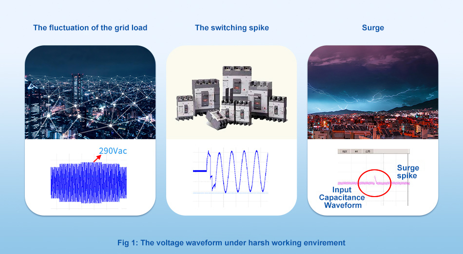
The input overvoltage is caused by the large fluctuation of the grid load. For example, the voltage is often low during peak power consumption and high when equipment is shut down.
The actual variation range of power grid voltage amplitude varies greatly with the power grid capacity, the transmission and distribution equipment quality, the power consumption, and other factors. In cities and industrial areas with a sound power supply, the variation range is usually only about ± 15% (The maximum value does not exceed 264VAC). If exceeds 264VAC, the power supply may be damaged, or even cause equipment trip and fire, threatening safety and property.
However, in countries and regions with poor power supply conditions, or on occasions where there is equipment with large load changes in the power grid, such as mountain areas, highway tunnels, charging stations, generator power supply, etc., the change range is much larger, sometimes even up to 20%~30% (The maximum value is up to274~299VAC).
Voltage stress analysis of power supply components under input overvoltage
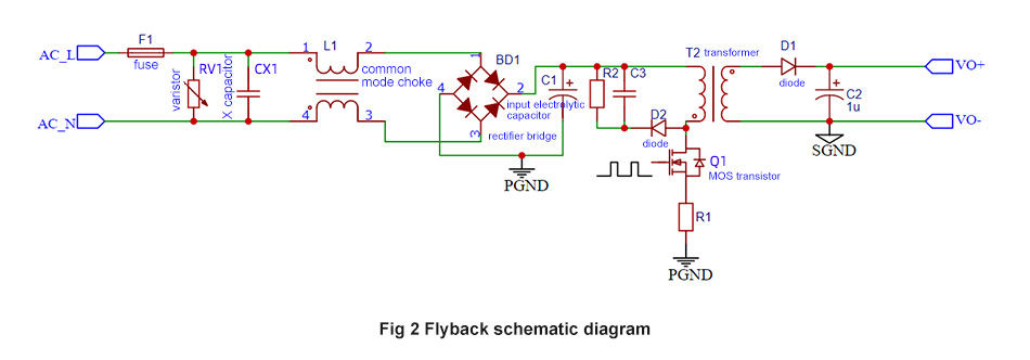
Take the flyback AC/DC switched-mode power supply in Figure 2 as an example to analyze how to select appropriate components according to the voltage stress when the input voltage reaches 305VAC.
1. Nominal voltage selection of fuse F1
The nominal voltage of the fuse must be greater than or equal to the maximum voltage of the turn-off circuit. Due to the very low resistance of the fuse, its nominal voltage becomes important only when attempting to fuse. When the fuse element melts, the fuse must be able to quickly disconnect, extinguish the arc, and prevent the open circuit voltage from triggering the arc again through the disconnected fuse element.
The common specifications of fuses are 125V, 250V, 300V, and 400V. In response to the large fluctuation of input voltage, a 300V fuse shall be selected.
2. The selection of rated voltage of varistor RV1
In practical application, varistor RV1 is generally connected in parallel in the circuit. When the circuit works normally, it is in a high resistance state, which does not affect the normal operation of the circuit. When the circuit has abnormal instantaneous overvoltage and reaches its turn-on voltage (varistor voltage), the varistor quickly changes from a high resistance state to a low resistance state, discharges the instantaneous overcurrent caused by abnormal instantaneous overvoltage, and clamps the abnormal instantaneous overvoltage within a safe level, so as to protect the subsequent circuit from the damage of abnormal instantaneous overvoltage.
Common specifications of varistor are as follows:

The voltage value of the varistor shall be greater than the voltage peak in the actual circuit, which means the power supply voltage continuously applied to both ends of the varistor shall be less than the "maximum continuous operation voltage value(AC and DC)" in the varistor specification. As shown in the table above, 300VAC(385VDC) obviously does not meet the long-term operation of 305VAC. In order to prevent damage to the varistor, it is necessary to select 10D561 varistors in case of large input voltage fluctuation.
3. Nominal voltage selection of X capacitor CX1
The nominal voltage of the X2 safety capacitor is generally 275V, 305V and 310V, which are actually universal. Because of the different nominal voltage requirements in the different countries and different safety regulations, the label of X2 is different. For example, the nominal voltage required for CQC certification in China is 310VAC, while that in other countries is 275V, 305VAC and 310VAC. In the case of large input voltage fluctuation, a 310V X-capacitor is preferred.
4. Nominal voltage selection of bridge rectifiers BD1
When Vin=264VAC, the maximum stress of the bridge rectifier diode should be Vmax1=264×√2=373V.
When Vin=305VAC, the maximum stress of the bridge rectifier diode should be Vmax2=305×√2=431V.
Since the switching power supply needs to do the lightning surge test, the rectifier bridge that is greater than 600V is generally selected. In order to meet the harsher surge environment, the 1000V rectifier bridge also can be selected.
5. Nominal voltage selection of electrolytic capacitor C1
When Vin=264VAC, the maximum stress of the electrolytic capacitor should be Vcmax1=264×√2=373V.
When Vin=305VAC, the maximum stress of the electrolytic capacitor should be Vcmax2=305×√2=431V.
In the case of large fluctuations in the input voltage, a 450V electrolytic capacitor should be selected.
6. Nominal voltage selection of MOS transistor Q1
The voltage stress of the MOS transistor equals VIN +VOR+VPK.
Vmos=VIN +VOR+VPK.
VIN refers to the input voltage, and the maximum input voltage is 431V. VOR is the reflection voltage, generally, 60-120V, which is positively correlated to the side turn ratio of original and secondary and output voltage, and can be taken as 80V or less through optimal design. VPK is the peak voltage generated from inductance, generally around 100V, and can be taken as 80V or less by optimizing leakage inductance and absorption parameters.
Therefore, the working voltage stress of MOS transistor Q1 should be 431+120+100=651V. After optimization, the working voltage stress of Q1 could be 431+80+80=591V. Therefore, considering the surge or 305VAC input, and in order to ensure the reliable operation of the MOS transistor, at least a 700V MOS transistor should be selected, but a 650V MOS transistor can also be selected after optimizing the turn ratio and leakage inductance of the transformer.
7. Nominal voltage selection of diode D1
The computational formula of voltage stress of the Diode is 
VD-PK refers to the peak voltage generated by the secondary leakage inductance. Since it is greatly affected by different output voltages and absorption parameters, it is generally calculated as 
Assuming that the output voltage is 12V(VO=12V), the leakage inductance peak of the diode is 30V( VD-PK=30V) and the MOS transistor leakage inductance peak of the MOS transistor is 80V(VPK=80V), the calculation is as follows:
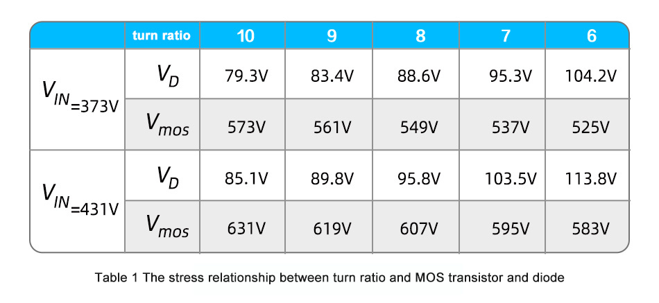
It can be seen from table 1 that the conventional AC/DC switching power supply only considers an input voltage of 373V(VIN =373V), and the values of the MOS transistor and diode will be relatively small, which cannot be applied to the input voltage of 431V. Once the input voltage exceeds 373V, there is a risk of damage.
To sum up, taking the output voltage of 12V as an example, in terms of the surge or input of 305VAC, in order to ensure the reliable operation of the diode, at least 150V diodes should be selected, but 100V diodes can also be selected by optimizing the turn ratio and leakage inductance of the transformer.
Protection requirements for input overvoltage
According to the calculation in PartⅡ, the best way to deal with input overvoltage is to optimize the voltage stress of components, such as components selection of MORNSUN 305RAC(Reliable under all conditions) power supplies.
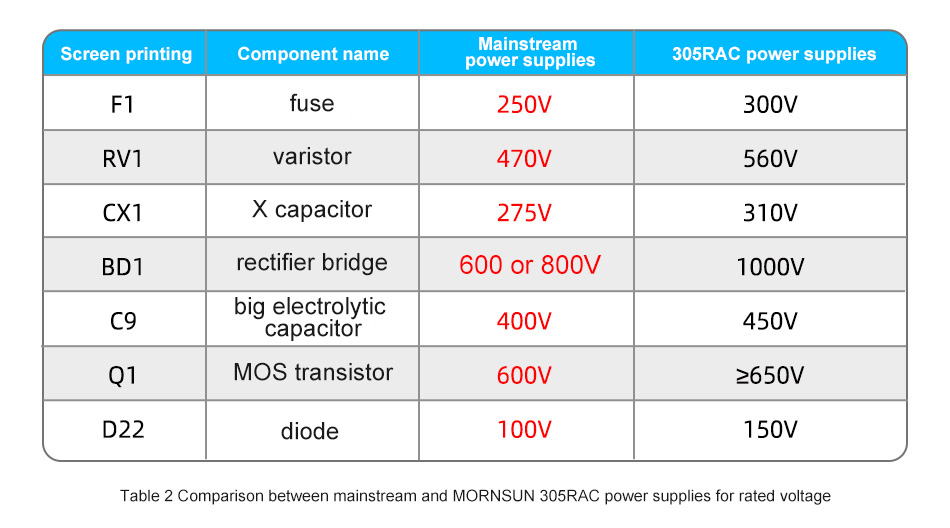
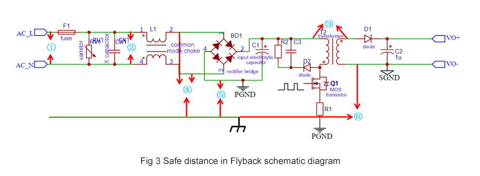
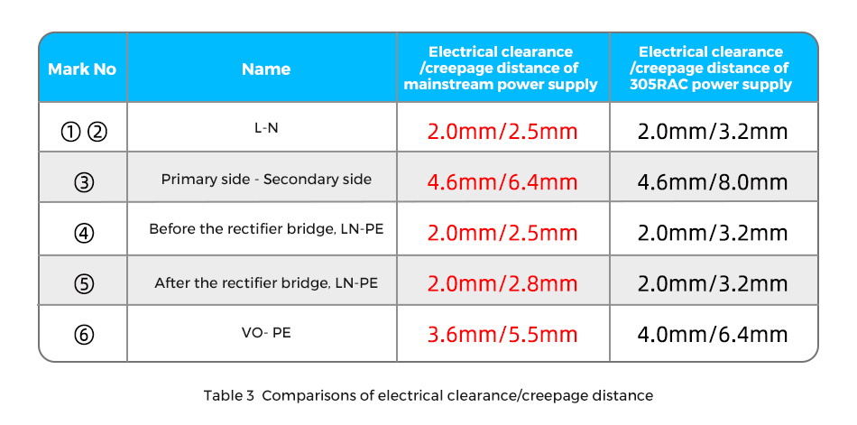
At the same time, keeping a safe distance between high-voltage lines can be maintained by increasing the internal electrical gap and creep distance, avoiding arcing damage to the prototype or endangering people's safety.
Summary
The input overvoltage will damage the power supply and cause harm to people. How to avoid input overvoltage? Through the voltage stress analysis of the power supply components, the selection guide of the key components of the AC/DC switched-mode power supply is determined. At the same time, increasing the internal electric gap and creep distance of the power supply is also beneficial for optimizing the voltage stress.
By comparing the rated voltage, electrical gap and creep distance of components between the mainstream power supply and the MRONSUN "305 RAC" power supply, the 305 RAC AC/DC power supply features effectively protect against input overvoltage. It can also be used in harsh and special environments with higher requirements in working temperature and humidity, altitude, EMC interference, etc.


